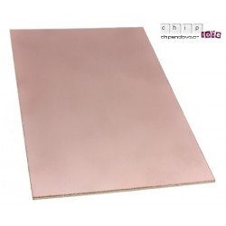
sourcing map Double Face Cuivre Stratifié Plaqué PCB Circuit
PDF 4.89 Mo - Industrie Canada

Double-sided PCB Manufacturing. 2 layer PCB

Ceta 2023, PDF, Circuit imprimé
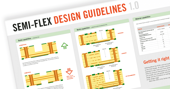
Multilayer PCB - technical specification
Description: *Parfait pour construire un prototype de circuit électronique, d Ouble PCB en cuivre côté. *Supporte et connecte électriquement des

sourcing map Double Face Cuivre Stratifié Plaqué PCB Circuit Imprimé FR4 200x200mm 7.87x7.87 pouce, 1.5mm Épaisseur Bricolage Prototypage PCB Carte
Description: *Parfait pour construire un prototype de circuit électronique, d Ouble PCB en cuivre côté. *Supporte et connecte électriquement des

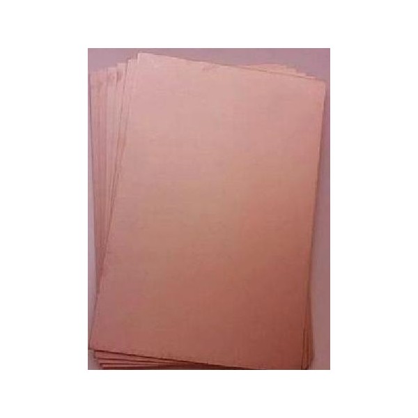
sourcing map Double Face Cuivre Stratifié Plaqué PCB Circuit Imprimé FR4 150x100mm 5.91x3.94 pouce, 1.5mm Épaisseur Bricolage Prototypage PCB Carte
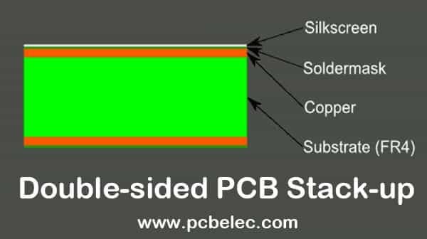
Double-sided PCB Manufacturing Process Flowchart and Step by Step
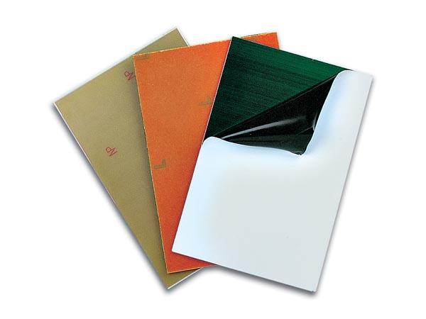
This double sided copper clad laminate pcb circuit board is great for etch etching project. Its bottom plate is uniform in color and smooth in

Copper PCB Board, 2Pcs Double Sided Copper Clad Circuit Board Laminate Blank PCB Copper Pads 20x30cm 1MM
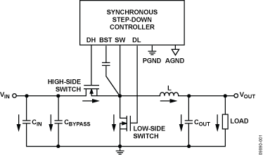
AN-1119: Printed Circuit Board Layout Guidelines for Step-Down Regulators, Optimizing for Low Noise Design with Dual Channel Switching Controllers [Analog Devices Wiki]
Multi-Layer PCB Standard Laminated Structures

An Introduction to 2 Layer PCB - RAYPCB
Multilayer PCB - technical specification